Nanjixiong's introduction: Ceramic 3D printing is moving rapidly from R&D toward industrial adoption. As photopolymer ceramic printing becomes a mainstream process across more applications, attention is shifting from proof that a part can be printed to stable, repeatable production of high-performance parts. The semiconductor industry uses large numbers of ceramic components, and several product iterations are bringing ceramic AM deeper into its supply chain.
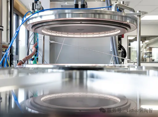
△ FALP chamber-lid assembly with a large-diameter gas distribution ring (image: Plasway Technologies)
In November 2026, Nanjixiong learned from Lithoz that it had completed several ceramic 3D-printing applications in the semiconductor industry:
- Germany's Plasway Technologies, Alumina Systems, and Lithoz jointly developed a 500 mm alumina ceramic gas distribution ring used in the same chamber for plasma-enhanced atomic layer deposition (PEALD) and atomic layer etching (ALE). Compared with a conventional metal-ring solution, continuous equipment operation increased from one month to nine months, and productivity rose about threefold.
- Sintokogio (formerly Bosch Advanced Ceramics) and an end customer are using Lithoz's ceramic photopolymerization printer to produce 1,000 ceramic gas injectors per year.
What does the ring do?
The main case is a 500 mm, dual-channel alumina gas distribution ring developed by Plasway Technologies with Alumina Systems and Lithoz. It is installed on Plasway's FALP (Fast Atomic Layer Processing) platform.
Atomic layer deposition (ALD) and atomic layer etching (ALE) are opposing steps: ALD coats surfaces layer by layer to protect trenches, while ALE precisely removes material layer by layer. They use different temperature windows and plasma parameters. FALP aims to alternate the two processes in the same chamber without breaking vacuum or transferring the wafer. The challenge is gas management: precursors and co-reactants must remain completely separated before entering the chamber, form symmetric laminar flows at the wafer surface, and be rapidly evacuated after reaction.
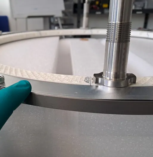
△ FALP's adjustable-diameter mounting mechanism and integrated stainless-steel gas inlet
According to Plasway founder and CEO Stephan Wege, conventional showerhead geometries have dead zones where gas does not exchange quickly enough and precursors may react prematurely, making that approach unsuitable.
The platform demonstrates the process with specific figures. ALE first removes the native oxide from a silicon wafer. It then deposits a 10 nm aluminum-oxide insulating layer, a 14 nm titanium-nitride conducting layer, a 10 nm silicon-oxide insulating layer, and a second 14 nm titanium-nitride conducting layer. The four-layer stack is completed in 15 minutes without breaking vacuum.
Why use ceramic 3D printing?
The ring integrates two non-intersecting internal flow paths and computationally optimized Laval nozzles. Slip casting, ceramic injection molding, and dry pressing cannot produce this one-piece geometry. The material is 99.9% high-purity alumina. Alumina Systems says the chamber contains strong plasma and corrosive gases that can erode a metal ring within months, while high-purity alumina can withstand long-term use.
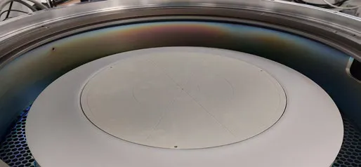
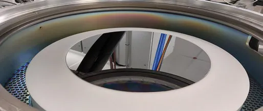
△ Bipolar electrostatic chuck (ESC) developed for 300 mm wafers: (top) the chuck and wafer-support structure for precise temperature control in the FALP chamber; (bottom) the chuck with a loaded wafer
The surrounding system also matters. A 3,600 L/s turbomolecular pump is positioned symmetrically at the center of the chamber to ensure uniform purging across the wafer. With an 18-inch ring and a 17-inch substrate, non-uniformity in silicon-dioxide film deposition remains around 3%.
Wege says that replacing the conventional metal ring with the ceramic 3D-printed gas distribution ring increased stable continuous operating time from one month to nine months and tripled overall productivity.
Four generations in four years: from a 380 mm prototype to a 500 mm production part
The development was not achieved in one step. The four product generations illustrate ceramic 3D printing's transition from prototype to production.
- 2018, first-generation 380 mm ring: the main ring was still made by conventional slip casting, while only its nozzles were printed on Lithoz equipment. It was installed on a validation tool at Dresden's IKTS. The concept worked, but Wege acknowledged that the composite structure could not be mass-produced; the turbomolecular pumps were arranged asymmetrically, causing uneven gas flow when gas was shut off.
- Second generation, one-piece ring: the entire ring was printed by ceramic photopolymerization, removing the joint between the ring and nozzles. Production challenges then included demolding a large green body, sintering distortion, and handling.
- Third generation, segmented ring: Lithoz proposed dividing the 380 mm ring into six segments, sintering each separately, and joining them with Alumina Systems' glass-sealing process. This improved printing precision, yield, and debinding efficiency. Gas uniformity can be tested on each segment, and a failed segment can be discarded without waiting for the entire ring to finish sintering.
- Fourth generation, 500 mm ring: the customer needed a 430 mm substrate, so the number of segments increased from six to eight. Two stainless-steel gas inlets were integrated into the ceramic ring. The FALP system was paired with a proprietary bipolar electrostatic chuck, with temperature, plasma density, and ion energy controlled independently in closed loops. Lithoz also optimized CeraFab build layouts: three years ago, one S65 build could produce only four segments; now a CeraFab S320 can produce 14 per build, nearly two complete 500 mm rings. Wege praised Lithoz's large-format adaptation and the precision with which it controlled alumina-slurry shrinkage.
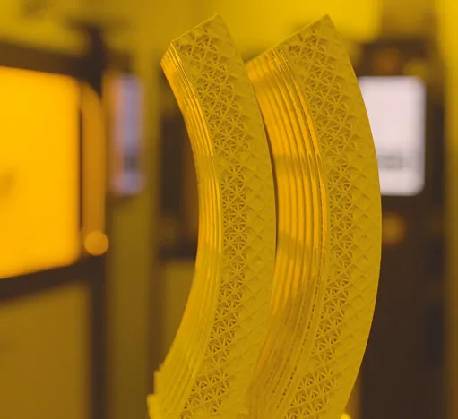
△ One S320 build can produce 14 segments, increasing production efficiency for the 500 mm distribution ring.
Quality inspection follows the segmented process. Before joining, each segment undergoes an individual gas-uniformity test, dye-penetrant crack inspection, and UV scanning. Non-conforming parts are discarded—“engineering ceramics cannot be repaired once cracked”—before the ring is assembled and installed.
Sintokogio Advanced Ceramics: production capacity of 1,000 parts per year
Ceramic 3D printing is not an isolated semiconductor application. Sintokogio Advanced Ceramics and an end customer used Lithoz's photopolymer ceramic-printing process to redesign a gas injector for an etch chamber. A two-piece assembly was integrated into one ceramic part containing three 6 mm-diameter channels and 62 flow-optimized outlet holes. The minimum wall thickness is 0.2 mm, forming accuracy is 40 μm, and the material is 99.8% alumina (LithaLox 350). Flange tolerance is ±0.1 mm.
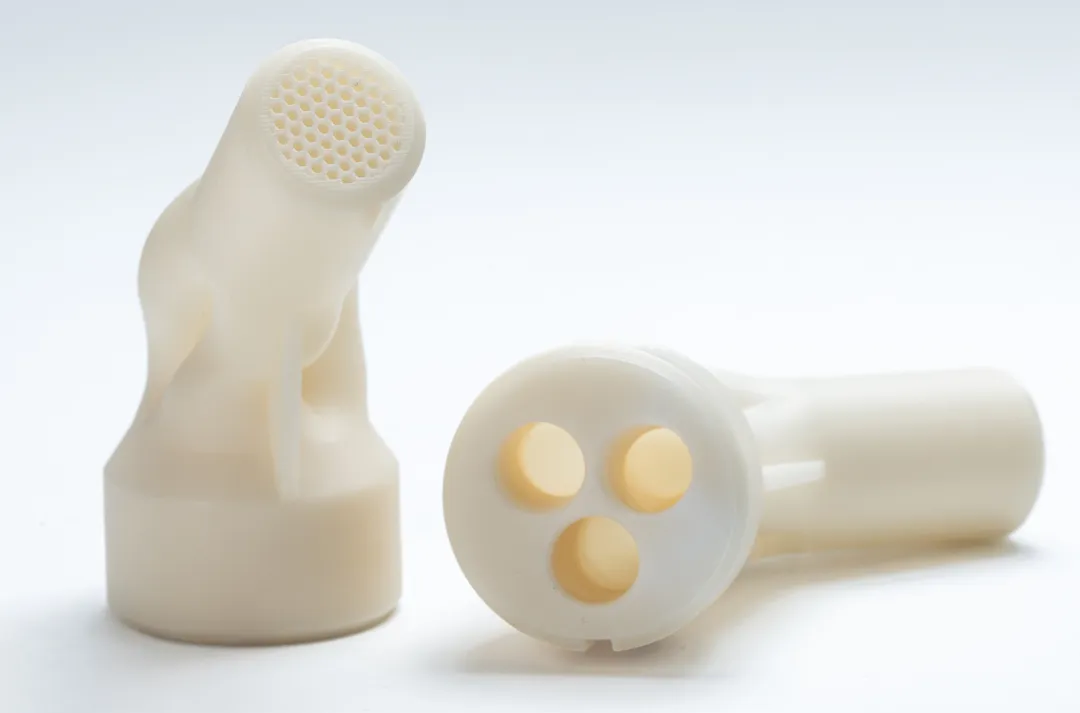
△ 3D-printed ceramic gas injector (image: Sintokogio Advanced Ceramics)
The part is now in production at 1,000 units per year, with six parts produced per build. Sintokogio Chief Strategy Officer Ashu Sharma gave a practical rationale: metal parts shed particles in corrosive conditions, while plastics degrade in plasma. Semiconductor production lines are especially sensitive to particle contamination. Ceramic 3D printing also eliminates assembly misalignment as a possible failure source. The company developed its own green-body cleaning process, since removing slurry from complex internal cavities without damage is another hidden prerequisite for production.
Lithoz to exhibit in Germany at Formnext
Lithoz will show new systems and several applications at Formnext this year, Hall 11.0, booth B50.
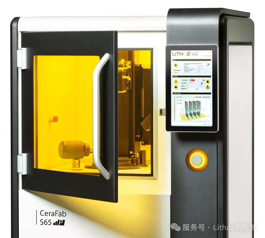
CeraFab S65 with 4K optics: the build area remains nearly unchanged, while resolution improves from 40 μm (635 dpi) to 25 μm (1,016 dpi) and light intensity rises from 60 mW/cm² to about 120 mW/cm². For ceramic 3D printing, doubling light intensity is more important than resolution alone: dark slurries have long been a challenge for photopolymerization, and the increase makes black zirconia and other dark ceramics printable.
One full build of aluminum-nitride cold plates: a single S320 can produce 116 heat-exchanger plates in one build. Aluminum nitride has thermal conductivity of 211 W/(m·K) and a thermal-expansion coefficient close to silicon. It is attracting interest for advanced packaging, power modules, optical modules, and CPU/GPU cooling. Conventional cold plates are made by machining two pieces and sealing them; 3D printing can form complex channels in one piece, improving sealing and heat-exchange efficiency. Japan's Mitsui Mining & Smelting is already using 3D-printed aluminum nitride for oil-cooled heat exchangers.
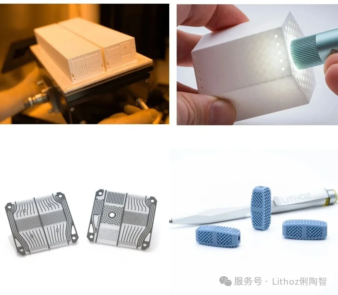
Other examples include ceramic casting cores for turbine blades from Germany's Access; an alumina cold plate metallized with molybdenum-manganese for Sigma; blue-black zirconia watch bezels; hydroxyapatite interbody fusion devices developed with Swiss company Spherene; a spiral solid-oxide fuel-cell single cell from the Technical University of Denmark with a power-to-weight ratio of 1 W/g versus 0.2 W/g for conventional planar cells; topology-optimized rocket components developed with Leap71; and lead-free piezoelectric KNN parts.
Nanjixiong's view
Ceramic 3D printing has often been justified by geometric complexity. These cases tell a different story: in semiconductor equipment, the value lies in two capabilities together—continuous operation for months in a harsh plasma environment, and yields and throughput that keep pace with the production line. Equipment is progressing toward higher resolution, larger build areas, and darker slurries, while materials are expanding into systems with real demand, including aluminum nitride, zirconia, hydroxyapatite, and lead-free piezoelectrics.
Plasway has already scheduled its next step: a four-chamber production system is planned for the fourth quarter of 2026, with capacity four times higher than its current single-chamber system. For Chinese ceramic 3D-printing manufacturers, the benchmark is changing. It is no longer only about printing an impressive sample, but about getting parts into a German equipment maker's bill of materials and running on a customer's production line month after month.
AI-translated from an article by Xiaoruanxiong on Nanjixiong, originally published on 2026-11-11. Text and images retain the original source attribution.
Read the original Chinese article |


 Record number | ©2024 panda3dp Team. Powered by panda3dp