

848
|
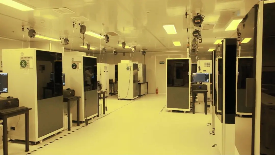
As a leading force in China’s 3D printing industry, Shanghai Prismlab Technology Co., Ltd. (hereinafter referred to as “Prismlab”) has been rooted in the digital dentistry sector since its founding in 2005, guided by the core philosophy of “solving personalized needs through industrialized solutions.” In collaboration with German chemical giant BASF, Prismlab has developed high-performance photopolymer resins, establishing a comprehensive solution that spans 70% of the dental materials product line. These innovations support mass production in dental applications such as invisible orthodontics and implant guides. Its 24-hour unattended ‘dark factories’ can produce 36 million customized dental molds annually, earning Prismlab the dual crown in the global dental 3D printing market.
This success in dentistry paved the way for Prismlab’s foray into the era of micro-nano manufacturing. Drawing upon its expertise in intelligent production, the company has turned its focus to ultra-high precision micro-nano 3D printing technologies. By leading the Ministry of Science and Technology’s national key R&D program, 'Additive Manufacturing Processes and Equipment for Micro-Nano Structures,' Prismlab has overcome micron-level fabrication challenges, achieving an unprecedented printing precision of 2 microns and boosting printing speed over a hundredfold compared to traditional processes.
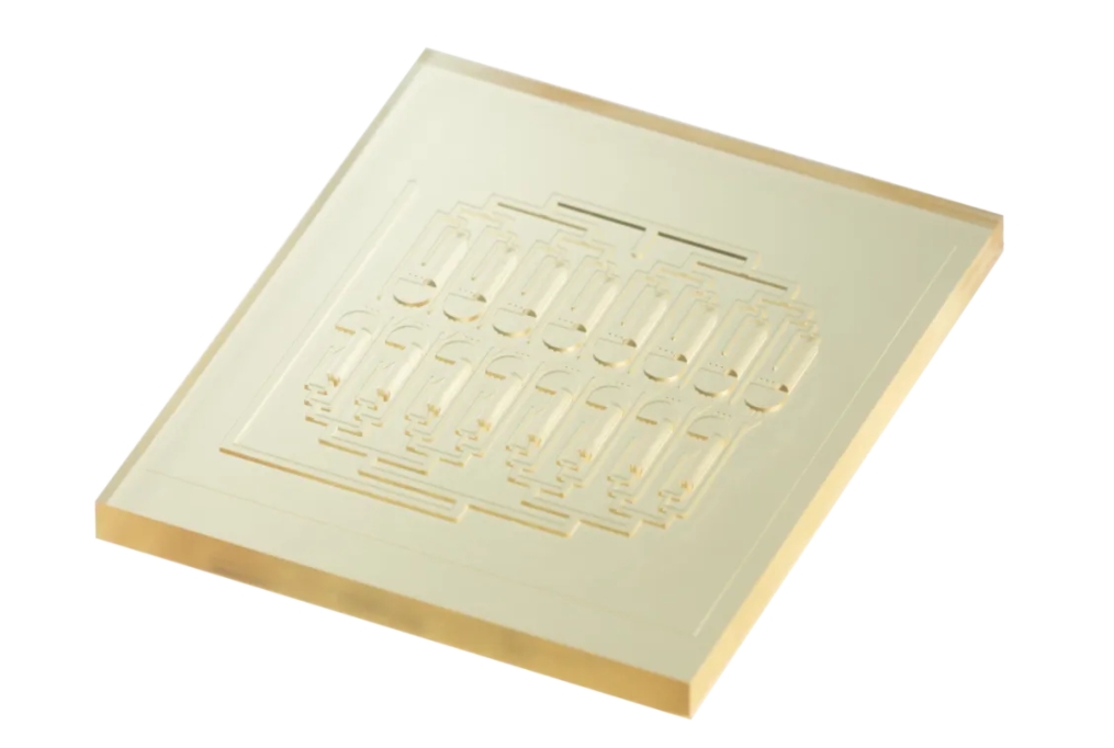
Core Advantages of Prismlab’s Micro-Nano 3D Printing
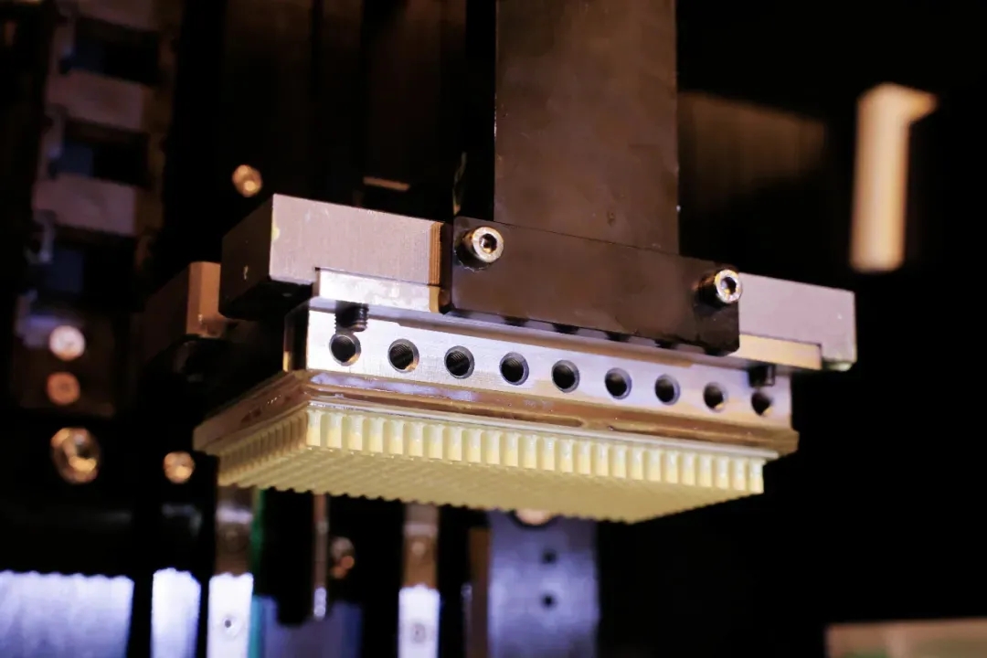
Prismlab’s technological edge lies in its independently developed Subpixel Micro-Scanning (SMS) technology, which marks a dual breakthrough in both speed and resolution:
- Seamless Full-Field Exposure: Unlike conventional 3D printing that requires multiple stitched exposures—prone to misalignment—Prismlab’s SMS uses a matrix-based exposure to complete intricate structures in a single pass, entirely eliminating stitching errors and increasing efficiency nearly a hundredfold.
- Ultra-High Speed Meets High Precision: With speeds tens of thousands of times faster than two-photon polymerization, the technology maintains a consistent resolution of 2 microns. It supports diverse materials such as resins, ceramics (e.g., alumina, zirconia), and metals (e.g., TC4 alloy, copper), meeting the complex demands of various industries.
- Fully Localized Industrial Chain: All core technologies and equipment are independently developed, with 67 domestic and international patents (including 10 international ones) and 100% localization of critical components.
Industrial Applications of Micro-Nano 3D Printing
Prismlab’s micro-nano technology has permeated cutting-edge fields such as healthcare, consumer electronics, and aerospace, cultivating a diversified ecosystem of applications:
1. Medical Field: A Paradigm Shift from ‘Minimally Invasive’ to ‘Precisely Engineered’
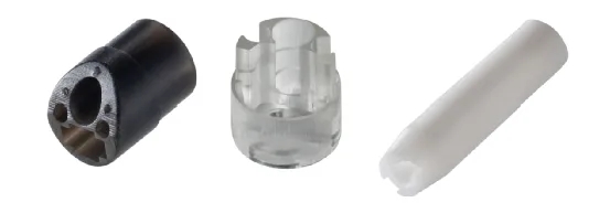
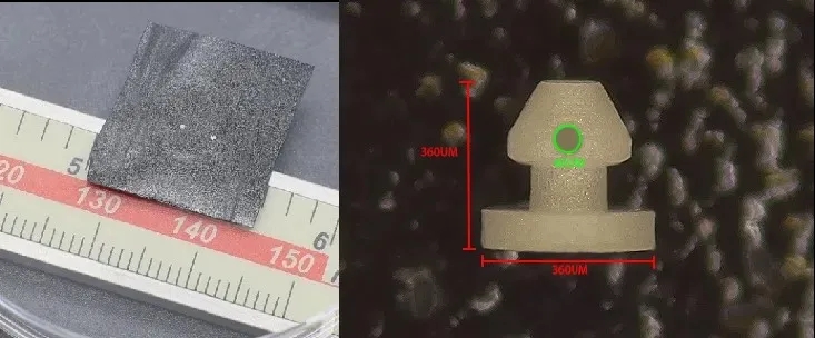
- Endoscopic Tips: Breakthrough construction of thin-walled channels with a 20:1 depth-to-diameter ratio, achieving 80-micron wall thickness while enabling multidimensional, interwoven internal networks. Using biocompatible materials like alumina, zirconia, and photopolymers, these tips allow rapid iteration and surpass traditional machining.
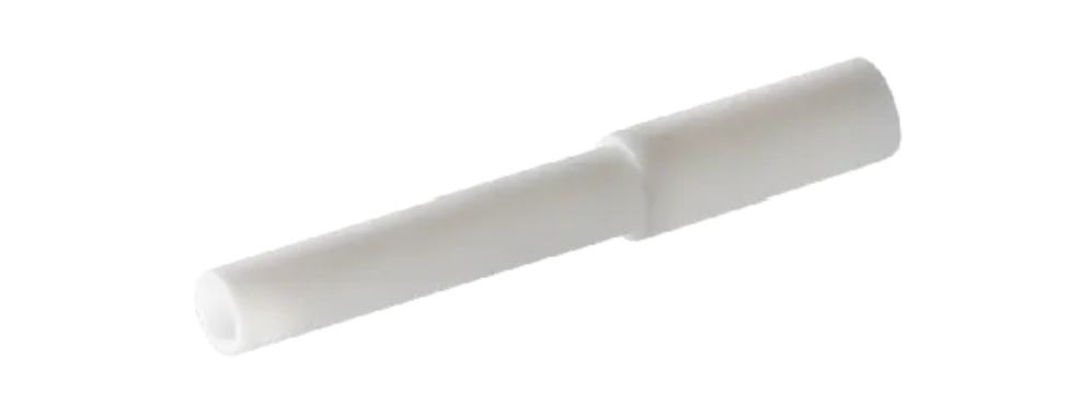
- Glaucoma Drainage Implants: Measuring under 400 microns, with apertures of 60–80 microns, these implants offer high strength and superior biocompatibility, ideal for minimally invasive ophthalmic procedures.
- Vascularized Organoid Chips: Co-developed with Shanghai Jiao Tong University, these organ-on-a-chip platforms simulate human microenvironments and facilitate targeted drug research, with results published in authoritative international journals.
- Microwave Ablation Tubes: Featuring 100-micron ceramic walls with high strength, breakdown resistance, and biocompatibility.
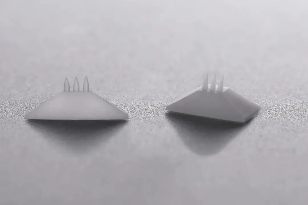
- Hollow Ceramic Microneedles: With a needle tip as fine as 3 microns, these enable painless transdermal delivery in cosmetic and medical applications (e.g., hyaluronic acid, collagen, insulin, vaccines), avoiding the breakage risks of traditional silicon microneedles.
2. Consumer Electronics: Empowering 6G Communications and Smart Devices
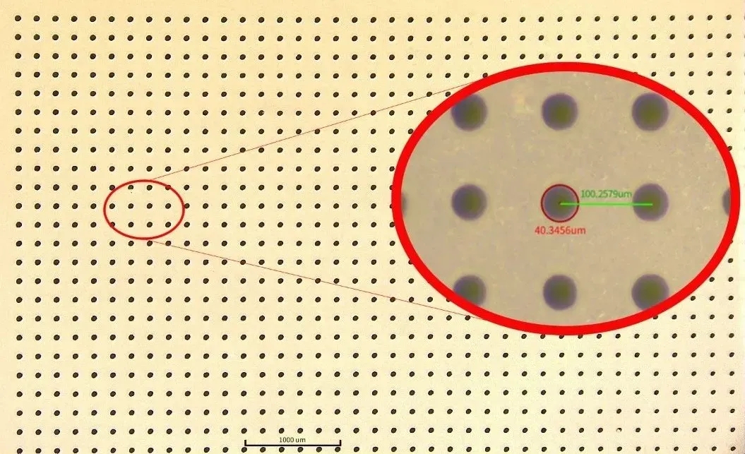
- Micro Displays and Brain-Computer Interfaces: Ceramic substrates as small as 1 cm² can host 10,000 micro-apertures (30 microns each), offering a precise platform for electrode arrays.
- Microfluidic Chips: Applied in biomedical testing and pharmaceutical R&D, enabling precise manipulation of microvolumes and improving testing efficiency more than threefold.
Future Outlook: Domestic Innovation Steers the Global Stage
Prismlab’s success validates its forward-thinking strategy of ‘mass-customizing precision through industrial means’—simultaneously addressing niche market needs and reducing costs at scale. As micro-nano technologies gain traction in brain-computer interfaces and targeted medicine, Prismlab is poised to emerge as a global standard-setter in precision manufacturing.
As Chairman Hou Feng aptly states, “Technological self-reliance is the sole passport to global competition.” In the arduous campaign for domestic technological sovereignty, Prismlab wields micro-nano innovation as a blade, forging a path for China’s high-end manufacturing to leap from follower to leader.
|

The plan is to deploy 2,000 3D printers for footwear researc

Priced Around CNY200/kg, Withstands Over 190°C Without Cham
Meituan Enters the 3D Printing Arena — Leads Series B Inves

Grab It for Just CNY17,000 — Consumer-Grade Continuous Fibe

BLT’s Metal 3D-Printed Car Body Parts and Brake Calipers He

Apple Recruits a 3D Printing Expert in Shenzhen — Requires

Shenzhen Hymson, a Laser Tech Firm Valued at Over 10 Billion
5 μm Layer Thickness Achieved — Yunyao DeepVision Redefine
AM news | Email:bd@nanjixiong.com
China 3D printing | Record number | ©2024 panda3dp Team. Powered by panda3dp
 News
News